LIO52 module
Overview
The LIO52 is a powerful, highly flexible, ultra-low power Bluetooth Smart module based on the nRF52832 SoC from Nordic Semiconductor. With an ARM® CortexTM M4F CPU, embedded 2.4GHz transceiver, and integrated antenna, it provides a complete RF solution with no additional RF design. Its small form factor makes it easy to integrate in any hardware design reducing development costs.
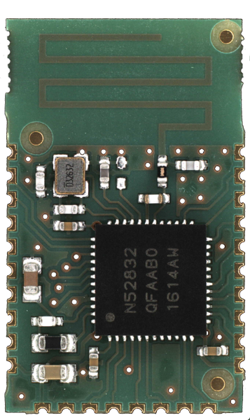
LIO52 module
Quick specifications
R.E.D certified
Bluetooth certified
Power supply: 1,7V – 3,6 with DC/DC regulator
Tx Power: +4dBm @ 7.5mA
Rx sensitivity: -96dBm @5.4mA
Power consumption: 0.3μA – 2μA (system off)
Memory: 512kB Flash & 64kB RAM
Integrated 32MHz crystal oscillator
Optional 32.768kHz external clock
20 General Purpose I/O Pins
Interfaces: SPI / UART / I2C / I2S / NFC / ADC / PWM
Dimensions: 21.1 x 12.7 x 2.7mm
Operating Temperature: -40°C to 85°C
Supported Firmware solutions
The LIO52 module comes with various firmware solutions answering most of needs :
LinkIO nRF BLE MESH built-in generic firmware with serial interface
LinkIO nRF BLE MESH built-in custom firmware (contact our sales)
LinkIO nRF SDK for developping embedded applications (contact our sales)
Detailed specifications
Processor
- ARM® Cortex™-M4 32-bit processor with FPU, 64 MHz
52 μA/MHz running from flash memory
48 μA/MHz running from RAM
Serial Wire Debug (SWD)
Trace port
- Flexible Power Management
Supply voltage range 1.7 V to 3.6 V
Fully automatic LDO and DC/DC regulator system
Fast wake-up using 64 MHz internal oscillator
0.4 μA at 3 V in OFF mode
0.7μA at 3 V in OFF mode with 32 kB RAM retention
1.9 μA at 3 V in ON mode, 32.768 kHz crystal oscillator and Real Time Counter running with 32 kB RAM retention
- Memory
512 kB flash/64 kB RAM
Radio
- 2.4 GHz transceiver
-96 dBm sensitivity in Bluetooth® low energy mode
1 Mbps, 2 Mbps supported data rates
RSSI (1 dB resolution)
- Radio current consumption DC-DC at 3V
7.5mA – TX at +4dBm output power,
5.3mA – TX at 0dBm output power,
5.4mA – RX at 1Mbs
Embedded features
Support for concurrent multi-protocol
Type 2 Near Field Communication (NFC-A) Tag with wakeup on field
12-bit, 200 ksps ADC - 8 configurable channels with programmable gain
64 level comparator
15 level low power comparator with wakeup
Temperature sensor
32 General Purpose I/O Pins
3 x 4 channel Pulse Width Modulator units with EasyDMA
Digital microphone interface (PDM)
5x 32-bit timers with counter mode
Up to 3x SPI Master/Slave with EasyDMA
2x I2C compatible 2-Wire Master/Slave
UART (CTS/RTS) with EasyDMA
Programmable Peripheral Interconnect (PPI)
Quadrature Decoder (QDEC)
AES HW encryption with EasyDMA
3x Real Timer Counter (RTC)
Pin Description
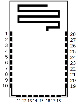
LIO52 pinout
Pin |
Name |
Type |
Description |
|---|---|---|---|
1 |
VSS |
Ground |
|
2 |
P25 |
General purpose I/O pin |
|
3 |
P26 |
General purpose I/O pin |
|
4 |
P27 |
General purpose I/O pin |
|
5 |
P28 - AIN4 |
General purpose I/O pin - ADC input 4 |
|
6 |
P29 - AIN5 |
General purpose I/O pin - ADC input 5 |
|
7 |
P30 - AIN6 |
General purpose I/O pin - ADC input 6 |
|
8 |
P31 - AIN7 |
General purpose I/O pin - ADC input 7 |
|
9 |
P2 |
General purpose I/O pin |
|
10 |
VDD |
DC supply |
|
11 |
VDD |
DC supply |
|
12 |
VSS |
Ground |
|
13 |
P0 - XL1 |
General purpose I/O pin - External 32.768kHz Chrystal clock |
|
14 |
P1 - XL2 |
General purpose I/O pin - External 32.768kHz Chrystal clock |
|
15 |
P3 |
General purpose I/O pin |
|
16 |
P4 |
General purpose I/O pin |
|
17 |
P9 - NFC1 |
General purpose I/O pin - Near Field Communication tag connector |
|
18 |
P10 - NFC2 |
General purpose I/O pin - Near Field Communication tag connector |
|
19 |
VDD |
DC supply |
|
20 |
P11 |
General purpose I/O pin |
|
21 |
P12 |
General purpose I/O pin |
|
22 |
P13 |
General purpose I/O pin |
|
23 |
P14 |
General purpose I/O pin |
|
24 |
P15 |
General purpose I/O pin |
|
25 |
P21 - RESET |
General purpose I/O pin - Programmable RESET pin |
|
26 |
SWDCLK |
HW debug and flash programming I/O |
|
27 |
SWDIO |
HW debug and flash programming I/O |
|
28 |
VSS |
Ground |
Mechanical data
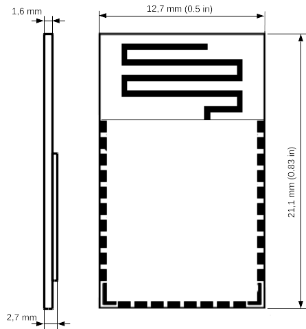
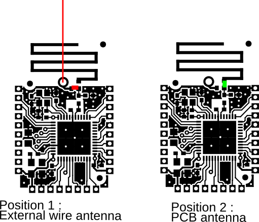
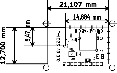

Module position And Antenna guidelines
The antenna is sensitive to any electromagnetic field close to it. So it needs to be as far as possible of the following element: Buck/boost converter, PWM, power signal (ex: mosfet of PCB2), filtering inductors, Triac, relays, …. . Moreover the antenna should be away by minimum 5mm from any other metal part (shield, live wire, PCB ground plane, PCB thick trace). It is sometimes impossible to follow these rules because of volume specification. But these rules need to be in mind for the placement and routing of the PCB. The most sensitive part of the antenna it the tip. It should be known that putting any kind of plastic, silicone,… will also have an impact so if the antenna needs to be held in place it should be the part near the base of the antenna and not the tip. Design the mechanicals and the enclosure around the antenna, not vice-versa. Antennas are paramount for radio performance. Therefore, the mechanical design of wireless embedded devices must serve the needs of the antenna. Not the other way around. Empty space is good space for the antenna. Many mechanical engineers and industrial designers want to build products in which every single square centimeter within each device is used. You need volume around the antenna for it to radiate, however, so your designs must have enough space, especially considering your ground plane requirements. Ensure your ground plane is large enough to meet your efficiency and bandwidth performance targets. Everything affects antenna performance. Nearly everything in small, wireless, embedded devices will conduct some RF current, which means the entire system is part of the antenna. This is a vital consideration. When designing custom antennas, we run electromagnetic simulations to project the RF currents on everything in the model—the ground plane, the battery, the connectors, the cables, LCD cans, shields, etc. They propagate to every piece of metal or any conductor within small devices. With everything part of the antenna, the key takeaway is you must tune the antenna in situ—in the final system configuration—to ensure the best performance. Antenna placement is essential. Keep antennas away from batteries, LCDs, cables, and EMI generators. Avoid conductors, absorbers, and dielectrics, which will detune the antenna, affect radiation patterns, and reduce efficiency. If the device is intended to be worn on the body, keep the antenna as far away from human tissue as possible. Placing switching power supplies close to the antenna will severely degrade receiver performance. Locating even a great antenna next to a noise generator will degrade system performance. Often, when customers complain about antenna issues, the problem is not the antenna but an electronics issue. There is simply too much EMI (noise) within the device that is radiating into the antenna and raising the noise floor at the receiver.
Effect of Enclosure and Ground Plane on Antenna Performance
Antennas used in consumer products are sensitive to PCB RF ground size and the product’s plastic casing. The antenna can be modeled as an LC resonator whose resonant frequency decreases when either L (inductance) or C (capacitance) increases. A larger RF ground plane and plastic casing increase the effective capacitance and thus reduce the resonant frequency
Effect of Ground Plane
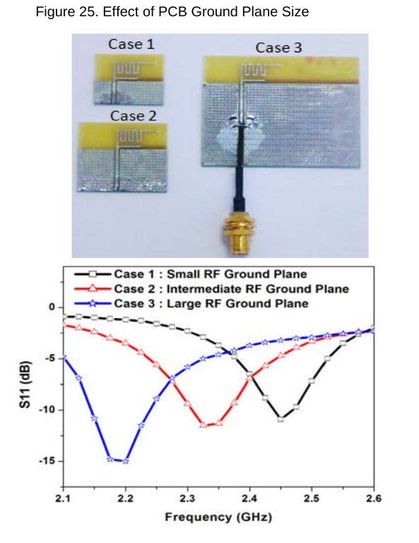
As explained before, a monopole PCB antenna requires a ground plane for proper operation. Figure 25 shows an example where a MIFA is placed on a PCB with a different ground plane size. The PCB size varies from 20 mm × 20 mm to 50 mm × 50 mm. The curves show that larger RF ground planes decrease the resonant frequency and better grounding provides better return loss. This is the key for a good PCB layout. The better the ground provided for the quarter-wave antenna, the better it will correlate with the theoretical behavior. This is a key concept in antenna design for small modules where there is hardly enough space for ground clearance.
Effect of Enclosure
Similar to the effect of the ground plane, to quantify antenna sensitivity to the product’s plastic casing, experiments were performed on a wireless mouse as shown in Figure 26. The Cypress MIFA is placed inside the plastic casing of the wireless mouse, and then measurements are made for radiation pattern and return loss. Both Figure 25 and Figure 26 reveal some important observations:
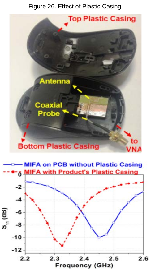
The resonant frequency shifts to a lower frequency when the antenna is placed near the plastic casing.
The shift in resonant frequency is observed to be about 100 MHz to 200 MHz. The antenna must be tuned again to bring it to the desired band. For antenna tuning, see Guidelines for Antenna Placement, Enclosure, and Ground Plane. In conclusion, increasing the ground plane size and plastic casing tends to decrease the resonant frequency of the antenna by approximately 100 MHz to 200 MHz.
Guidelines for Antenna Placement, Enclosure, and Ground Plane
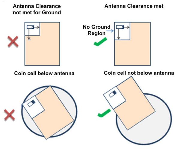
Always place the antenna in a corner of the PCB with sufficient clearance from the rest of the circuit.
Always follow the antenna designer’s/manufacturer’s recommended ground pattern for the antenna. Commonly used PCB antennas are variants of a monopole antenna. Monopole antennas need solid ground for proper operation.
Never place any component, planes, mounting screws, or traces in the antenna keep-out area across all layers. The actual keep-out area depends on the antenna used.
Do not place the antenna close to the plastic in the industrial design. Plastic has a higher dielectric constant than air. Proximity of the plastic to the antenna results in the antenna’s seeing a higher effective dielectric constant. This increases the electrical length of the antenna trace and reduces the resonant frequency.
The battery cable or mic cable must not cross the antenna trace.
The antenna must not be covered by a metallic enclosure completely. If the product has a metallic casing or a shield, the casing must not cover the antenna. No metal is allowed in the antenna near-field.
The orientation of the antenna should be in line with the final product orientation so that the radiation is maximized in the desired direction.
There must not be any ground directly below the antenna.
There must be enough ground at a distance (ground clearance) from the antenna and this ground plane must have a minimum width.
Plan to have a provision for an antenna matching network because a lot of parameters in the antenna’s proximity (plastic, ground variation, substrate differences, and other components) can vary its impedance, and therefore, the antenna may need retuning. If the impedance of the antenna is unknown, it is preferable to have a provision for a PI or T network of three components, with 0 ohms populated in series components and no load for shunt components. This helps you to populate any topology needed for a matching network later.
When using the matching network values provided by the antenna manufacturer, ensure that you use the trace length from the antenna to the matching network specified in the manufacturer datasheet or reference design.
Always verify the antenna matching network with the final plastic enclosure in place and the product placed in typical use case scenarios. For example, verify a mouse with its plastic held on the hand and placed on a mouse pad, plastic, wood, metal, or floor.
To resume:
Avoid any component that produces eletromagnetic emission near the antenna
Clear area near the antenna tip (at least 5mm clearance)
Avoid putting any kind of plastic, silicone, etc … on the antenna to avoid tuning out the antenna.
References:
Revision date : Mar 28, 2020